Subscribe to RSS
August 29, 2018
Go for the Triple Three!
Prof. Hiroshi Amano of the Nagoya University Institute of Materials and Systems for Sustainability wants to transform the world through electronics. To achieve this goal, the world's largest research laboratory of its kind was recently completed in a corner of Meidai's Higashiyama Campus. The blue light emitting diode (LED) developed by Prof. Amano together with University Prof. Isamu Akasaki triggered a global revolution in lighting and also earned them the Nobel Prize. However, the gallium nitride (GaN) from which it is made has even greater potential: It is a strong candidate material for next-generation semiconductors with high-performance and energy-efficiency that will play a crucial role in realizing a "super smart society" where everyone can live in safety and comfort.
At the new research laboratory, Prof. Amano aims to do "the full gamut" from basic research all the way to commercial application. But while the participation of private business is crucial to this endeavor, industry-academic partnerships in Japan are not faring so well, even as many Japanese companies are investing large sums of money in collaborations with overseas universities. Of course, Japanese universities are partly to blame, admits Prof. Amano. So, what to do?
Building a one-of-a-kind research laboratory is the first step, of course. But the question is how to get businesses to use it. Leveraging its strengths from pioneering the global development of GaN blue LEDs, Meidai has embarked on another grand mission: to transform global society by pioneering the development of next-generation semiconductors as well.
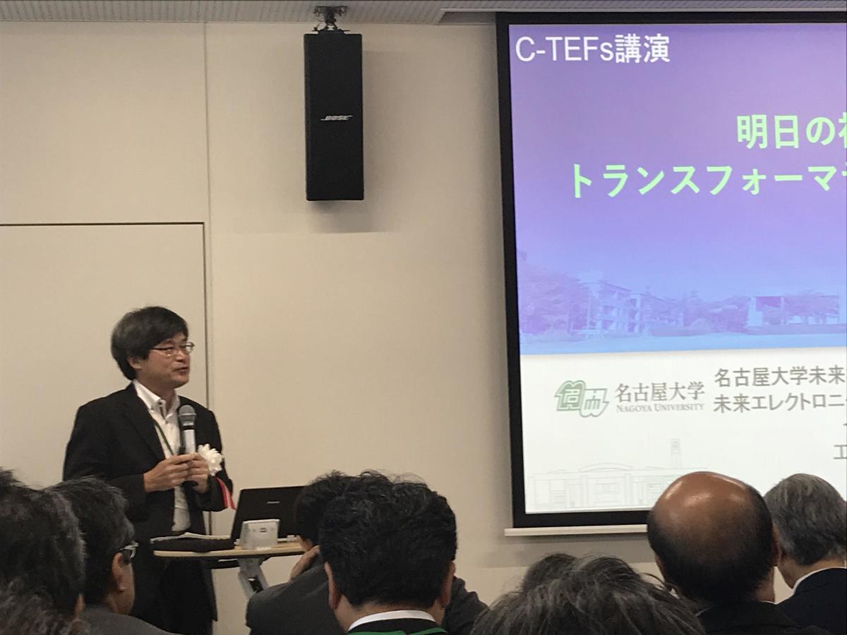 Prof. Hiroshi Amano speaking at the opening ceremony
At the opening ceremony for the CIRFE Transformative Electronics Facilities (C-TEFs) held at the end of July, Amano delivered a talk titled "Transformative electronics as a basis for future society", wherein he listed factors that contributed to success in the development of the blue LED. The first was that GaN was a unique solution. The second was the leadership of University Prof. Akasaki, who inspired younger researchers with his firm belief. And the third was the vitality of the manufacturing industry at the time.
How about now? First, as a next-generation semiconductor material, GaN possesses functional characteristics not found in other materials. It is also a unique solution. On the second point of leadership, Prof. Amano chuckled, "Let's set that aside for now." On the third point, Amano expressed the need in today's languishing industry to create innovation through collaboration between the public, private, and academic sectors. The number of research articles published in Japan has been declining for some twenty years now, and that decline is particularly notable in the business sector.
The new research laboratory contains a 1,000-square-meter cleanroom for carrying out the entire series of processes from growing high-quality crystals as material for semiconductors, to actually fabricating and evaluating devices like transistors. This is the largest cleanroom in the world dedicated to GaN. The Consortium for GaN Research and Applications, founded to advance research on the national level, currently counts 20 universities, 4 research institutions, and 47 companies as members. By the end of the year an adjoining research building will be completed and will provide companies with their own space. The plan is to provide everything necessary for prototype creation, the first phase of actual product development. A deep chasm lies between research and development and the marketing of a product, one so difficult to traverse it is also called the "valley of death." Amano aims to overcome it by bringing together the respective strengths of industry, academia, and government.
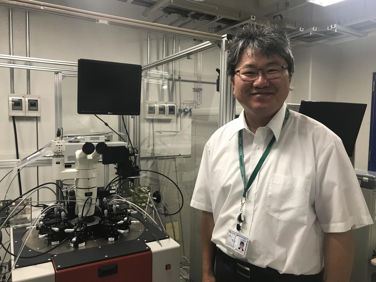 C-TEFs director Jun Suda has moved away from home to be at Meidai. On weekdays he immerses himself in work, and on weekends he returns home to spend precious time with family.
C-TEFs' leadership team was recruited widely from outside Meidai. Director Prof. Jun Suda moved to Meidai last year from Kyoto University, where he had spent 30 years, including his undergraduate years. As a student, Suda focused on zinc selenide (ZnSe), which was considered the strongest candidate for blue LEDs and the topic of much research worldwide. At the time, ZnSe was considered on the verge of commercial viability, while GaN posed numerous challenges and was believed would take more than two decades before reaching that point. However, in 1993, just two years later, Shuji Nakamura at Nichia Corporation succeeded in commercializing the GaN blue LED based on the research of University Prof. Akasaki and other; companies around the world switched to GaN. After graduation, Suda moved to the laboratory of Prof. Hiroyuki Matsunami, who was the first to develop a power semiconductor used in power control from silicon carbide. Following Matsunami's strong preference for doing the entire process from growing SiC crystals to evaluating their physical properties to fabricating devices, Suda carried out SiC research while, on the side, pursuing his own research on growing crystals and developing power devices with GaN, his old rival. Suda was well known at Meidai as he conducted joint research on GaN crystal growth with Akasaki and Amano.
Suda was thus the natural choice as C-TEFs director. Almost no one else possessed the critical experience of having worked on the whole sequence from crystal growth to device fabrication. Suda declined the offer multiple times, stating a preference for his own style of doing research with a small group of talented individuals. Nonetheless, "The paperwork for making me director proceeded quietly," he laughs. Now as head of the laboratory, he's ambitious: "At Meidai, the birthplace of GaN research, I want to make C-TEFs the world's leading institution for exploring the limits of all of GaN's possibilities."
SiC is GaN's biggest rival when it comes to next-generation semiconductors used for power devices. It already has a major lead, having been chosen for adoption in a bullet train in 2020, for example. Suda, who also spent many years in SiC research and development, says, "The characteristics required from power semiconductors vary widely depending on the application, and SiC is not omnipotent in this sense. Depending on the cost, GaN could even come from behind and hit a homerun."
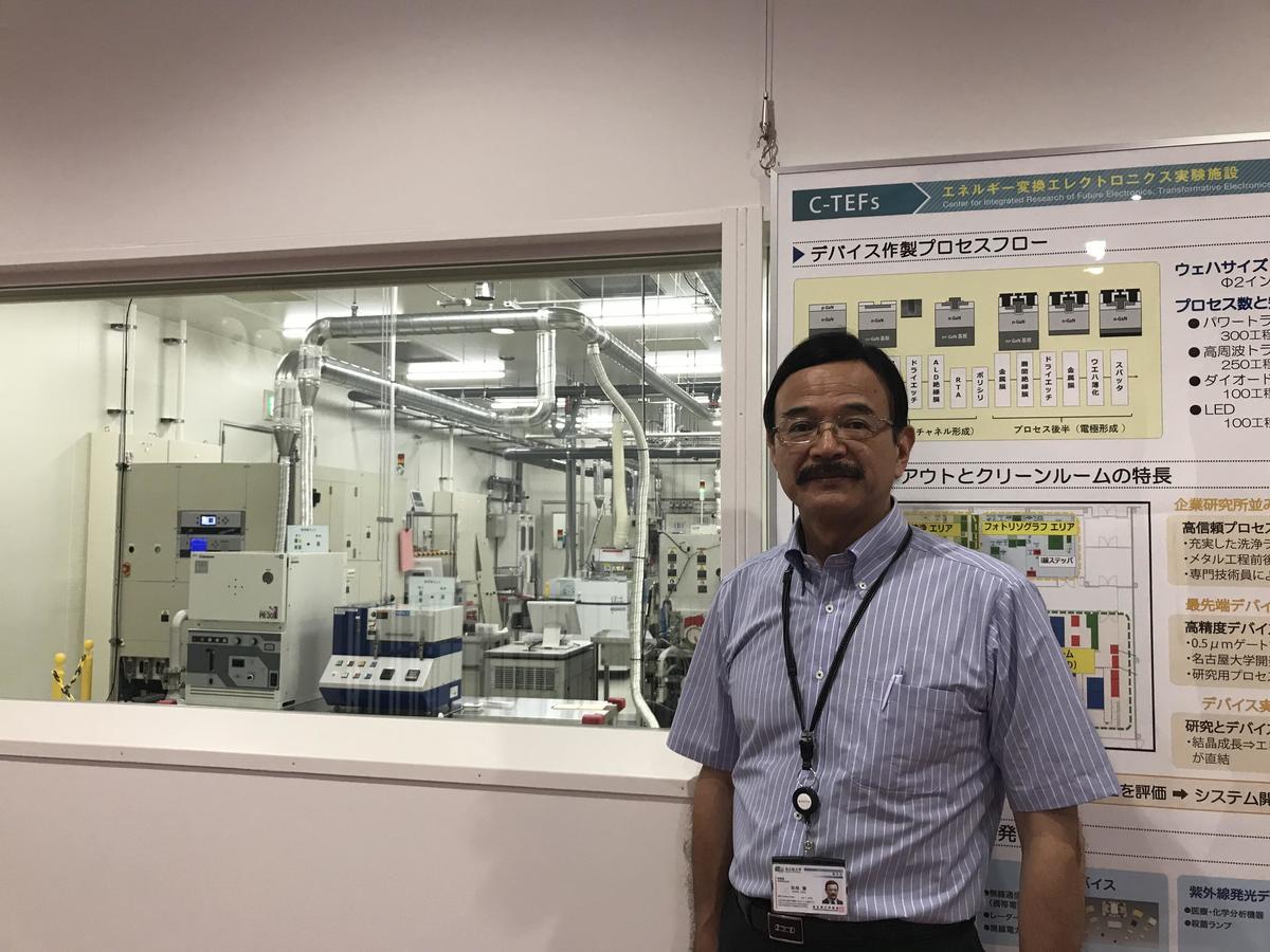 Designated Professor Tetsu Kachi standing in front of the cleanroom
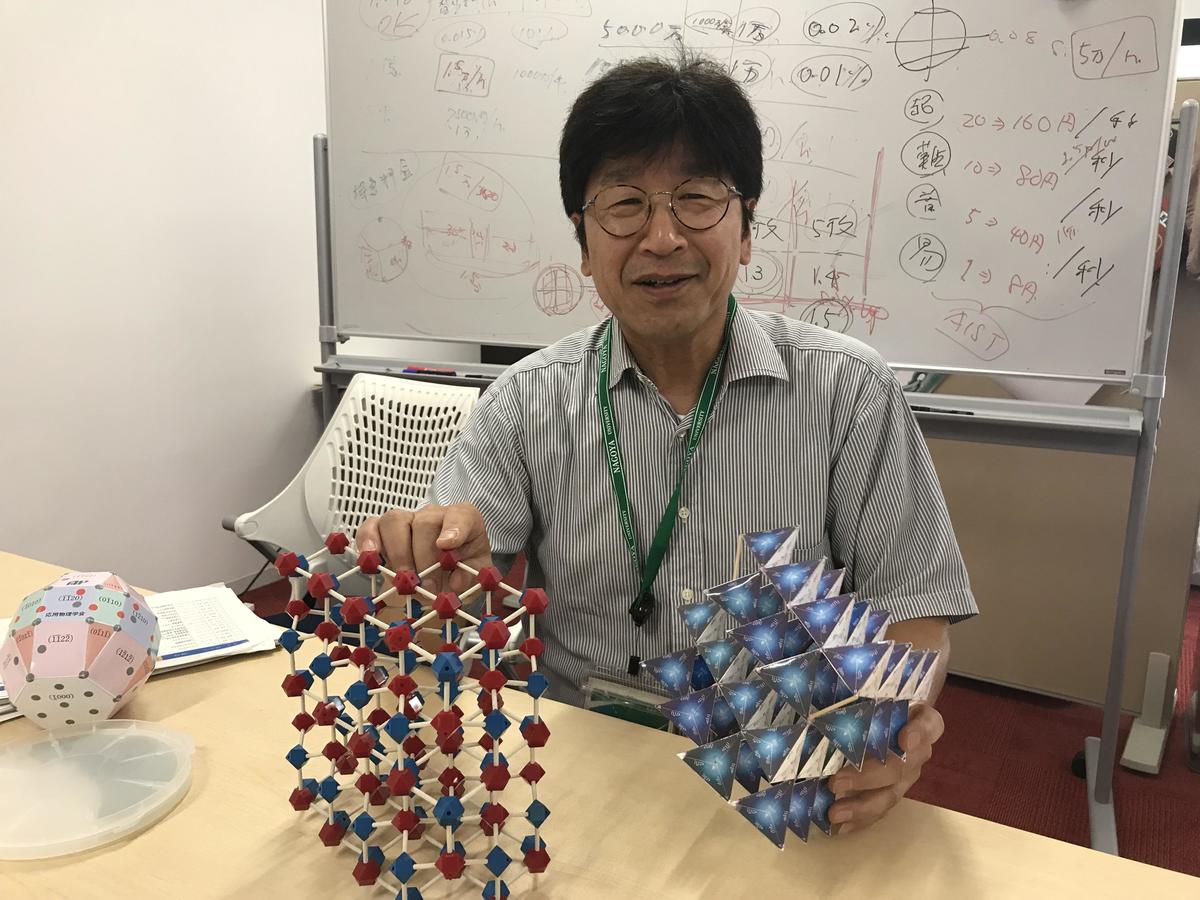 Designated Professor Shoichi Onda talks with crystal models in hand.
To the vice director posts, two veterans from leading automotive companies were appointed: Shoichi Onda from Denso Corporation and Tetsu Kachi from Toyota Central R&D Labs, Inc. (Toyota CRDL). Both are designated professors more than a decade older than Suda; Suda calls them "Suke-san and Kaku-san," after the samurai duo from the popular period drama Mito Komon. Both graduated from Nagoya University School of Engineering and were rivals in the field of automotive semiconductors at their respective companies, Onda leading research and development of SiC, and Kachi leading research and development of GaN.
However, when Toyota decided to adopt SiC for next-generation semiconductors about a decade ago, Toyota CRDL shrank its GaN program, and Kachi continued to do research on the smallest budget ever before heading into retirement. For him, the recent appointment was thus an unexpected return to center stage. What's more, he also convinced Toyota CRDL to provide on a special basis its "recipe" for making GaN devices, which comprises some 200 steps. It's a secret that under normal circumstances would never leave the company, even though development was halted. As a result, the C-TEFs team shocked those attending the opening ceremony by showcasing a device fabricated at the new facilities so quickly. With companies tending to view academic research in Japan as "playing pretend," researchers at C-TEFs left a strong impression that they mean business.
As both professors from company recognize, Japanese companies have in more than a few cases formed agreements with top overseas universities, especially in the U.S., totaling tens to hundreds of millions of yen (millions of dollars), while investing hardly any money in Japanese universities. According to a survey by the Japan Ministry of Education, Culture, Sports, Science and Technology, in 2014 Japanese companies made approximately 22,700 investments in Japanese universities, about two-thirds of which amounted to less than 3 million yen (about $27,000). Investments in overseas universities averaged about 11 million yen ー a stark difference.
Institutional differences are part of the reason. In the U.S., professors pay their doctoral students' salaries and tuition, so participating in faculty projects is effectively a student obligation. As a result, such projects are more likely to deliver results commensurate with the contract's value. In Japan, students pay their own tuition, and while this can mean more freedom, it also makes them less reliable in fulfilling agreements. In many cases, professors of Japanese universities are not viewed by companies as partners who will deliver sure results.
At the same time, overseas companies are often the first to notice and incorporate the outstanding achievements of Japanese universities; Japanese companies tend to be late to the game. A well-known example is the transparent oxide semiconductors developed by Prof. Hideo Hosono at Tokyo Institute of Technology. These semiconductors were later commercialized in large-screen displays, but the initial inquiries all came from companies outside Japan. Another instance was when Prof. Kenji Shiraishi, a member of Meidai's GaN research team and an expert in computational science, announced research results that had great significance for device design. Intel responded by changing its strategy practically overnight. Of course, though a bit late, Panasonic later developed and adopted a better strategy than Intel based on Shiraishi's research results.
It seems difficult to conclude that the exceptional achievements in basic research by Japanese universities are being fully utilized in Japan. Japanese companies may be lacking the spirit of enterprise, a willingness to take on new interests. As the decline in research articles from business sectors illustrates, at a time when companies have fewer resources for research and development, there's no reason not to make better use of university research.
Kachi comments, "We probably also need some awareness on the part of companies to foster universities and enliven the whole system." Onda, noticing the fierceness with which China and other countries are catching up to Japan in GaN research, a field supposedly Japan's forte, states, "Our future depends on whether we can do truly innovative research in the new laboratory's designated area of basic research." More than anything, creative research is essential to pursuing partnerships with industry.
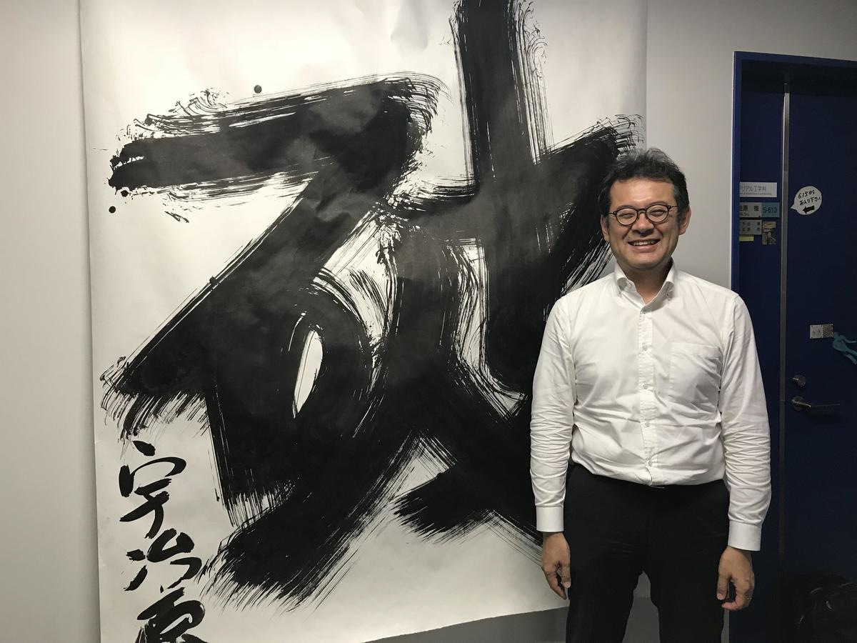 Prof. Toru Ujihara’s first calligraphy work of the year is “ha” (“accomplishment” in Japanese), representing his strong determination to succeed.
One thing even Prof. Amano has turned to as a potent tool in academic research is artificial intelligence (AI). Making high-quality crystals larger is essential to reducing the cost of semiconductors, but actual experiments to make crystals take a lot of time and effort. Indeed, it's taken 40 years to reach today's technology for silicon, currently the most common semiconductor material. Needless to say, that's too much time.
To address this, Prof. Toru Ujihara is working to simulate crystal growth using AI. While his background is in material science, Ujihara took an interest in AI through casual conversations with information researchers at Meidai, and spent three years studying AI with his students. With help from a Meidai-based IT startup, in short order he and especially his students became proficient at using AI as a tool. As a result, what used to take an hour or two they can now do instantaneously. In fact, their results indicate that the size of GaN crystals can be increased at a rate ten times faster than before.
"Universities have always fallen behind companies when it comes to completing things. If we could change that, companies will probably take us more seriously," says Ujihara. When, based on the crystal growth simulations, he developed a virtual reality technology that essentially offers a window into a nearly 2,000-degree-Celsius furnace, companies were impressed and calls immediately came in from overseas. He's also germinating some new seeds, including a new method of growing SiC crystals, and a technology that improves the thermal conductivity of plastics and keeps them from heating up. Next-generation semiconductors are expected to function in a wide range of applications, from automobiles to wireless charging, and when you include peripheral fields, there are innumerable problems to solve. "The game isn't over yet."
The new facilities will enter full operation next year. Their large size means more funding is required to keep them operating, but most of that is expected to be earned through user fees. The goal is to realize a positive feedback loop: The more companies use the facilities, the more income is generated and goes toward better maintenance, which encourages use.
The business model for the new facilities is the Interuniversity Microelectronics Centre (IMEC) in Belgium, known globally as a center of open innovation research in the semiconductor processing field. Companies gather there seeking the advantages of its cutting-edge laboratories and the ability to do research in emerging fields with academic researchers. Panasonic is one such company. The new technology based on the research of the aforementioned Prof. Shiraishi was also brought to life by a researcher while at IMEC.
Hiroyuki Sakaki, the recognized leader of semiconductor research and president of Toyota Technological Institute which is a member of the Consortium for GaN Research and Applications, applauds the completion of infrastructure similar to IMEC, but also raises an expectation: "C-TEFs should balance and integrate two components: the ability to reliably carry out the processes companies value, and the bold idea and other academic elements universities are best suited for." In pro baseball terms, the point comes down to having both home runs and a high batting average. And, like the "triple three" ― .300 batting average, 30 homeruns, and 30 stolen bases ― C-TEFs also needs to steal more bases. In other words, it needs speed.
My hope is for C-TEFs to create a new form of industry-academic partnership, in which the strengths of both sides ― academic and industry ― come alive. Go for the triple three!